
***This article is intended for non-commercial research and private study.
Introduction
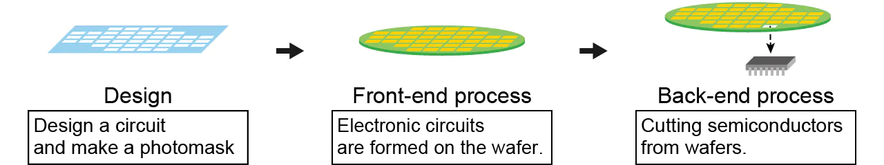
The semiconductor manufacturing process can be divided into three main areas: the design, front-end, and back-end processes.
In the design step, the circuit layout and specifications of the semiconductor chip are established.
In the front-end process, circuits are formed on the surface of the silicon wafer.
In the back-end process, preparations are made to cut and integrate the chips.
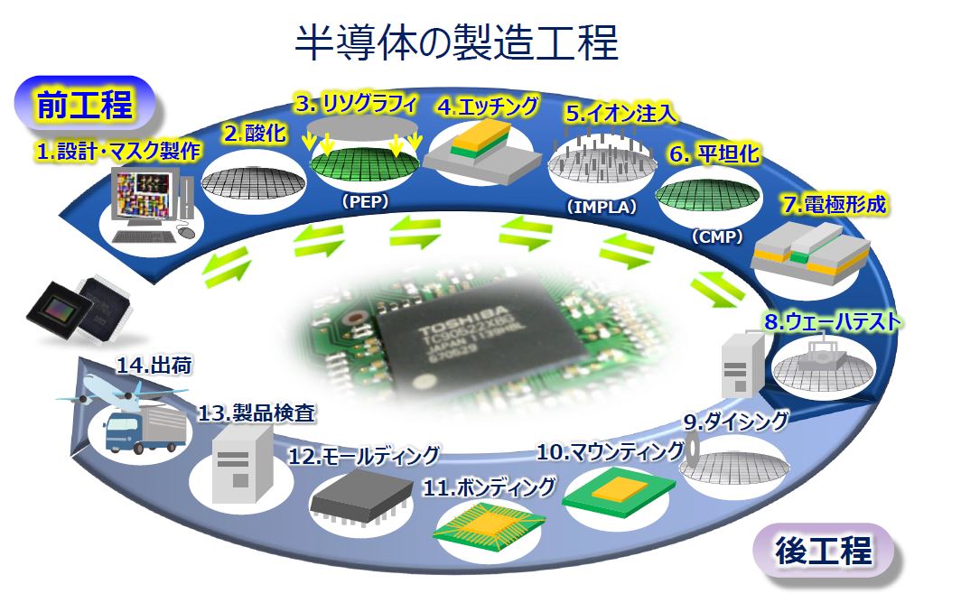
Some key steps involved in semiconductor manufacturing processes:
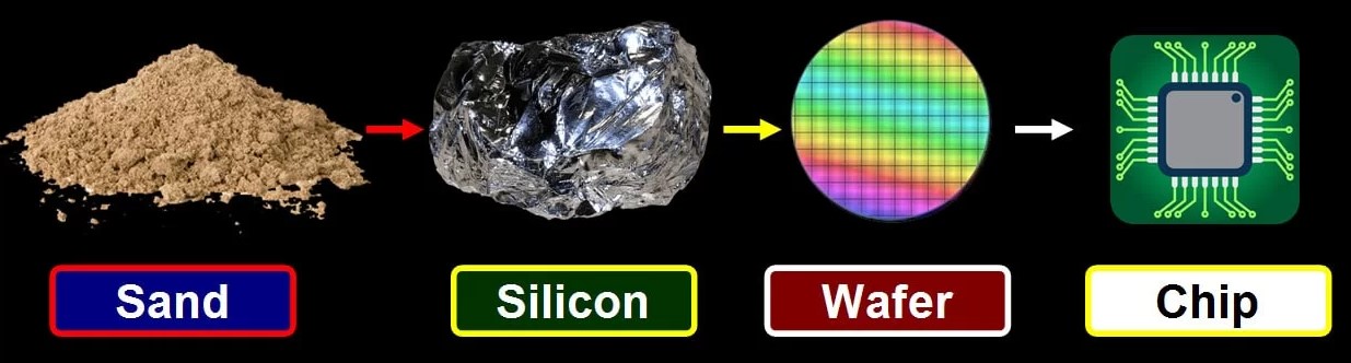
Wafer: Foundation for Semiconductor.
Oxidation: A thin layer of silicon dioxide (SiO2) is grown on the surface of the wafer through a process called oxidation. This oxide layer serves as an insulating layer and can also act as a mask for subsequent processes.
Photolithography: Draw Circuit Design on Wafer. A photosensitive material called a photoresist is applied to the wafer, exposed to light through a mask, and then developed, leaving a patterned resist on the wafer surface.
Etching: The exposed areas of the wafer, where the resist has been removed, are etched using either wet or dry etching techniques. This step selectively removes unnecessary material according to the patterned resist, defining the desired features on the wafer.
Dopant Implantation: Dopants, which are impurity atoms introduced intentionally to modify the electrical properties of the silicon, are implanted into specific regions of the wafer using ion implantation. This step allows the creation of n-type and p-type regions, forming transistors and other components.
Dopant Implantation: Dopants, which are impurity atoms introduced intentionally to modify the electrical properties of the silicon, are implanted into specific regions of the wafer using ion implantation. This step allows the creation of n-type and p-type regions, forming transistors and other components.
Deposition: Thin layers of various materials, such as metals, insulators, and semiconductors, are deposited onto the wafer surface through processes like chemical vapor deposition (CVD), physical vapor deposition (PVD), or atomic layer deposition (ALD). These layers form interconnects, gates, and other necessary structures.
Annealing: The wafer undergoes a high-temperature annealing process to activate dopants, repair crystal lattice damage caused by ion implantation, and improve the electrical characteristics of the fabricated devices.
Metallization: Metal layers are deposited and patterned to create interconnects, connecting the different components of the integrated circuit. Allows electricity to flow by depositing a thin metal film.。金属層を半導体表面に堆積させることで、トランジスタや抵抗器、コンデンサなどの様々な部品を接続する手段を提供します。
Testing: In the final stage of semiconductor manufacturing, the wafers are tested for functionality, performance, and reliability to ensure compliance with specifications, and defective items are removed to achieve completion.
Packaging: Good wafers are then cut into individual chips and packaged in protective casings, and pins are attached to establish external connections, and then ready for integration into electronic devices.
 Semiconductor Manufacturing Process flow